EN
EN  EN
EN DA
DA NL
NL FI
FI FR
FR DE
DE IT
IT JA
JA KO
KO NO
NO PL
PL PT
PT RO
RO RU
RU ES
ES SV
SV TL
TL ID
ID SK
SK UK
UK VI
VI TH
TH TR
TR FA
FA BE
BE LA
LA UZ
UZ

PSPI photosensitive polyimide photoresist
| Qhov chaw ntawm keeb kwm: | Tuam Tshoj |
| Hom Npe: | Semixlab |
| Model Number: | PSPI-01 |
| Certification: | ISO9001 |
| Yam Tsawg Tshaj: | Yuav tsum tau sib tham ua ntej |
| Nqe: | Tiv tauj rau Kev Hais Tus Nqi Tshwj Xeeb |
| Ntim Paub meej: | Pob khoom xa tawm txheem |
| Tus me nyuam lub sij hawm: | Lub Sij Hawm Xa Khoom: 15-30 Hnub Tom Qab Kev Pom Zoo |
| Ntsiab lus uas them: | T / T |
| Mov Muaj peev xwm: | 100 tons/Month |
Hauj lwm
Semixlab PSPI photosensitive polyimide packaging material
PSPI is a liquid photosensitive resin material for semiconductor manufacturers. It serves mutiple crucial functions in semiconductor production,acting as a surface protection film for semiconductor elements, a passivation layer for bumps, and an insulating layer for rewiring.
This material stands out due to its outstanding characteristics. It offers excellentheat - and chemical -resistance capabilities. Moreover, it boasts remarkableelectrical and mechanical properties.
To meet the evolving needs of the industry, we have developed a diverse productportfolio. These products are well - equipped to fulfill the requirements of next -generation packaging technology, ensuring that we can provide solutions thatkeep pace with the latest advancements in the semiconductor field.
Thov :
It is mainly used in the semiconductor field, for the surface protective film of semiconductor components, raised passivation layer, rewiring insulation layer and so on. It is also increasingly used in cutting-edge packages that require multi-layer formation.
Cov kev pabcuam uas muab tau:
kev tshuaj xyuas qhov xwm txheej ntawm cov neeg siv khoom siv, cov ntaub ntawv sib phim, kev daws teeb meem kev siv tshuab.
Company profile:
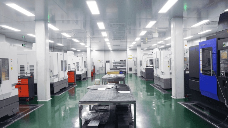
Semixlab muaj 2 lub chaw soj nstuam, ib pab neeg kws tshaj lij nrog 20 xyoo ntawm kev paub txog khoom siv, nrog R&D thiab kev tsim khoom, kev sim thiab kev txheeb xyuas.
Nthuav Qhia:
1. Different names for products:PSPI photosensitive polyimide photoresist/PSPI/Photosensitive insulating /PSPI photosensitive polyimide packaging material/Photosensitive Polyimide.
2. Main Application:It is mainly used in the semiconductor field, for the surface protective film of semiconductor components, raised passivation layer, rewiring insulation layer and so on. It is also increasingly used in cutting-edge packages that require multi-layer formation.Mainly in the field of medium and high Semiconductor packaging.
3. Core Specifications:
Photosensitive resolution ≤3um, thermal stability up to 320℃, dielectric constant 3.3 (1MHz), adhesion 40Mpa, strong acid and alkali corrosion resistance, narrow process window, mainly in the field of medium and high packaging.

Specifications
Product performance comparison table:
| Kev ntsuas ntsuas | Asahi Kasei (Japan) | Semixlab |
| Photosensitive resolution | ≤2 hli | ≤3 hli |
| Thermal stability (Tg) | > 350 ° C | 330 ° C |
| Dielectric constant (1MHz) | 3.1 | 3.3 |
| Adhesion (MPa) | 45 | 40 |
| Tshuaj ua hauj | Strong acid/alkali resistance | Medium corrosion resistance |
| Process window | Nqaim | Nqaim |
| Thov teb | High-end ntim | Mid-to-high-end packaging |
daim ntawv sau npe
Cov txheej txheem thov ib txwm muaj

Through the innovation of material molecular structure and optimization of process parameters, Semixlab PSPI has achieved breakthrough progress in domestic high-end packaging materials, providing reliable packaging guarantee for cutting-edge fields such as 5G RF modules, automotive-grade power modules, and AI chips. If you need to obtain detailed technical white papers or arrange sample testing, please contact our technical support team.
Kev Tshaj Loj (Competitive Advantage)
Semixlab PSPI Core Advantages
1. Ultra-high-precision lithography
3μm resolution to meet the needs of micro-bump and RDL routing for 2.5D/3D packages.
Steep and straight sidewall morphology (85°-88°) to enhance the reliability of multilayer stacking.
2. Extreme environmental stability
Glass transition temperature above 330°C to adapt to the high temperature packaging of power devices.
Low dielectric loss (Df<0.005) for high-frequency millimeter-wave scenarios Low dielectric loss (Df<0.005), suitable for high-frequency millimeter-wave scenarios.
3. Breakthrough in process compatibility
Supports i-line/g-line dual-band exposure, compatible with mainstream domestic lithography equipment.
Developing latitude ±15%, reducing the impact of process fluctuations.
4. Domestication of technological innovations
Independently developed "nano-crosslinking enhancement" technology, increasing mechanical strength by 30%.
Halogen-free environmentally friendly formulations in line with EHS international standards.
Cov cheeb tsam tseem ceeb:
| Kev Taw Qhia | Hom Scenario | Tus nqi ntawm kev daws teeb meem |
| Advanced Ntim | Fan-Out, SiP, Chiplet RDL Layer | High Density Interconnect + Ultra-thin Coating (<5μm) |
| Cov khoom siv fais fab | IGBT, SiC Module Passivation Layer | High Temperature Cycling Resistant (-55°C~250°C) |
| MEMS Sensors | Biochip Microstructure Protective Layers | Low Stress Deformation Control ( <50MPa) |
| Zaub Tsav Tsheb | Micro-LED Macro-Transfer Temporary Bonding Layer | Laser Debonding Response Sensitivity Optimization |
5. Eco-chain validation endorsement
Has passed the reliability certification of the head packaging and testing factories, such as Changdian Technology and Tomfool Microelectronics, and is suitable for SMIC's 55nm BCD process.
peb pab

Semixlab khoom khw