
 EN
EN  EN
EN DA
DA NL
NL FI
FI FR
FR DE
DE IT
IT JA
JA KO
KO NO
NO PL
PL PT
PT RO
RO RU
RU ES
ES SV
SV TL
TL ID
ID SK
SK UK
UK VI
VI TH
TH TR
TR FA
FA BE
BE LA
LA UZ
UZ


Etching Focus nplhaib
| Qhov chaw ntawm keeb kwm: | Tuam Tshoj |
| Hom Npe: | Semixlab |
| Model Number: | EFR-01 |
| Certification: | ISO9001 |
| Yam Tsawg Tshaj: | 1 set |
| Nqe: | Tiv tauj rau Kev Hais Tus Nqi Tshwj Xeeb |
| Ntim Paub meej: | Pob khoom xa tawm txheem |
| Tus me nyuam lub sij hawm: | Lub Sij Hawm Xa Khoom: 30-35 Hnub Tom Qab Kev Pom Zoo |
| Ntsiab lus uas them: | T / T |
| Mov Muaj peev xwm: | 600 teeb tsa / Hli |
Hauj lwm
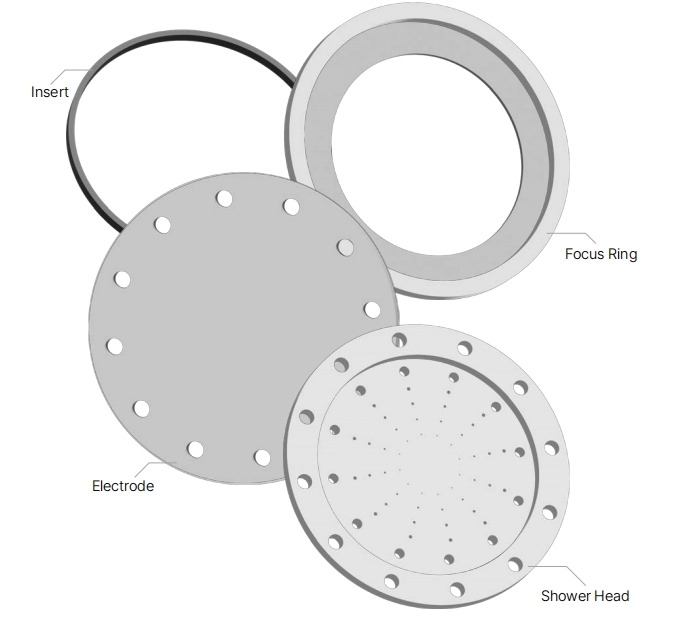
In core semiconductor manufacturing processes such as CVD chemical vapor deposition, etching, and thin film deposition, Etching Focus Ring (Etching Focus Ring), Electrode (Electrode), ETC (Edge Temperature Controller) and other consumable components are key components to ensure process accuracy and stability. These components are precisely assembled in a vacuum chamber to achieve uniform machining of nanoscale structures on the wafer surface through precise control of plasma distribution, edge temperature and electric field uniformity.
In response to the strict requirements of cleanliness and stability in high-end processes (such as 5nm and below), Semixlab has introduced etched focusing rings and supporting consumables with high-purity Monocrystalline Silicon as the core material, compared with traditional Quartz materials. Breakthrough in corrosion resistance, thermal stability and dielectric properties.
Core material comparison: monocrystalline silicon vs. Quartz
1. Plasma corrosion resistance
Monocrystals. Highly consistent with the wafer base material, they exhibited very low etching rates in fluorine-based (CF₄, SF₆) or chlorine-based (Cl₂) plasma environments and lived up to 3-5 times as long as quartz, reducing equipment downtime and replacement frequency.
Quartz: Although it has good high temperature resistance, it is easy to form micro-cracks under high-energy ion bombardment, resulting in an increased risk of particle pollution, especially in the long-term etching process.
2. Thermal conductivity and thermal expansion coefficient
Monocrystalline silicon: the thermal conductivity (149 W/m·K) is significantly higher than that of quartz (1.4 W/m·K), which can rapidly conduct process heat and reduce local thermal stress. Its low coefficient of thermal expansion (2.6×10⁻⁶/K) matches silicon wafers to avoid component deformation due to temperature fluctuations.
Quartz: low thermal conductivity, easy to form a temperature gradient in the chamber, affecting the plasma uniformity; The thermal expansion coefficient (0.55×10⁻⁶/K) is very different from that of wafer, which is easy to cause micro-displacement of components under long-term high temperature.
Dielectric properties and process accuracy
Monocrystal silicon: Very low dielectric loss (tanδ <0.001), the RF electric field distribution can be accurately regulated to ensure that the edge to the center of the wafer etching rate difference is less than 1.5%, meeting the requirements of advanced processes for line width uniformity.
Quartz: The dielectric constant (3.8) is different from the silicon-based environment, which easily leads to electric field distortion, and the edge effect is significant, which affects the forming consistency of the high aspect ratio structure.
Why choose monocrystalline silicon?
In advanced processes below 7nm, the Process Window is narrowed to the atomic scale, and the short life plate and electric field interference effect of traditional quartz consumables have become yield bottlenecks. With its physical and chemical homology with wafers, monocrystalline silicon material can significantly reduce interface interference, extend the maintenance cycle to more than 3,000 hours, and reduce the overall cost by 40%.
Nthuav Qhia:
1. Other names: Focus ring,Etching ring,Focus ring for etching,Monocrystalline silicon focusing ring.
2. Application: Isoconsumable components are key components to ensure process accuracy and stability. These components are precisely assembled in a vacuum chamber to achieve uniform machining of nanoscale structures on the wafer surface through precise control of plasma distribution, edge temperature and electric field uniformity.
3. Core parameters: Thermal conductivity (149 W/m·K), can quickly conduct process heat, reduce local thermal stress; Its low coefficient of thermal expansion (2.6×10⁻⁶/K) matches silicon wafers to avoid component deformation due to temperature fluctuations.
Specifications
Technical data comparision
| project | Monocrystalline silicon etching focus ring | Quartz etching focusing ring |
| purity | > 99.9999% | > 99.99% |
| Corrosion resistance life | 5000-8000 wafer passes | 1500-2000 wafer passes |
| Thermal shock stability | Tolerance ΔT>500℃/s | Tolerance ΔT<200℃/s |
| Nto saum npoo av | Rau <0.1μm | Rau <0.5μm |
daim ntawv sau npe
HAR Etching: In 3D NAND and TSV (through silicon) process, stable maintenance of deep hole side wall perpendicality.
Atomic Layer etching (ALE) : Removal of single atomic layers by precise electric field control to avoid over-etching.
Compound semiconductor processing: Low defect rate etching compatible with wide band gap materials such as GaN and SiC.

Kev Tshaj Loj (Competitive Advantage)
Zero pollution guarantee: The monocrystalline silicon material is ultra-precision polished (Ra <0.1μm) and Class 10 clean room package to avoid particulate matter release and meet the semiconductor grade cleanliness standard (SEMI F47).
Intelligent temperature control design: Integrated ETC module, real-time monitoring and adjustment of edge temperature through embedded thermocouple, compensation of process chamber thermal drift, to ensure batch repeatability.
Customized compatibility: Support customized aperture and thickness according to the client station model (such as AMAT Centura, Lam Research Kiyo), for a variety of plasma sources (ICP, CCP).


