
 EN
EN  EN
EN DA
DA NL
NL FI
FI FR
FR DE
DE IT
IT JA
JA KO
KO NO
NO PL
PL PT
PT RO
RO RU
RU ES
ES SV
SV TL
TL ID
ID SK
SK UK
UK VI
VI TH
TH TR
TR FA
FA BE
BE LA
LA UZ
UZ

Semiconductor quartz wafer nkoj
Nthuav Qhia:
1. Other names: Semiconductor quartz tank,quartz bath for semiconductor,quartz tank for semiconductor.
2. Application: The Semiconductor Quartz wafer boat for high temperature processes such as diffusion, oxidation, CVD, annealing, etc., in semiconductor manufacturing.
3. Cov txheej txheem tseem ceeb:
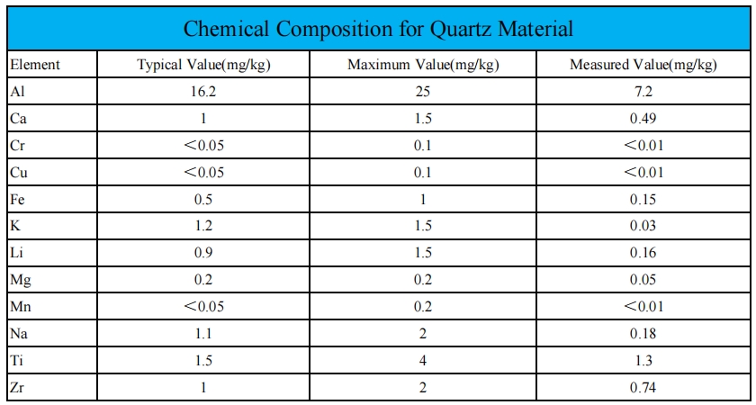
Ultra-high purity quartz (>99.99% SiO₂) : avoids contamination by metal ions (Na +, K +, Fe³+, etc.) and meets the cleanliness requirements of advanced processes (<5nm nodes).
High temperature resistance: continuous working temperature 1200℃, instantaneous temperature resistance 1300℃.
Chemically inert: Resistant to process gases such as HCl, H₂, O₂, SiH₄ and acid/alkaline environments. Non-corrosive for long-term use.
Hauj lwm
Semixlab Semiconductor Quartz wafer boats are key bearing tools designed for high temperature processes such as diffusion, oxidation, CVD, annealing, etc., in semiconductor manufacturing. Made of high purity synthetic quartz with excellent high temperature resistance, chemical stability and low thermal expansion coefficient, it can stably carry wafers in harsh process environments to ensure process consistency and product yield.
Applicable equipment: Compatible with all kinds of Horizontal/Vertical Diffusion Furnace (Horizontal/Vertical Diffusion Furnace), LPCVD system and rapid heat treatment (RTP) equipment.
Kev ruaj ntseg zoo
Strict quality control: 100% helium mass spectrometry leak detection (leakage rate <1×10⁻⁹ mbar·L/s). Material purity report (ICP-MS test) is issued for each batch.
Certification standards: In line with SEMI F47 specifications, through the ISO 9001:2015 quality management system certification.
Service life: the average life under normal conditions is more than 2 years (depending on process frequency and temperature conditions).
Why choose our quartz boat?
Customized services: Customized size and construction according to equipment model (TEL, Kokusai, ASM, etc.) and process requirements.
Fast response: Standard delivery time is 3 weeks, urgent orders can be reduced to 10 working days.
Global service network: Provide technical advice, installation guidance and after-sales maintenance support.Material Specifications.
Specifications
Qhov project specification
Material synthesis Fused Quartz
Purity ≥99.99% SiO₂
Wafer size compatibility 8 ", 12 "(can be customized 6" or 18 ")
Operating temperature ≤1200°C (continuous) / 1300°C (peak)
Coefficient of thermal expansion (CTE) 0.55×10⁻⁶/°C (20-1000°C)
Surface roughness (Ra) ≤0.2μm
Standard capacity 25/50/100 tablets
Applicable process gases O₂, N₂, H₂, Ar, SiH₄, HCl, etc
| Cov cuab yeej cuab tam | Density (g/cm3) | 2.2 |
| Mohs hardness | 6-7 | |
| Compressive strength (MPa) | 1100 | |
| Tensile strength (N/mm2) | 50 | |
| Flexural strength (N/mm2) | 65 | |
| Torsional strength (N/mm2) | 30 | |
| Young's modulus (MPa) | 7.2x10⁴ | |
| Poisson tus ratio | 0.16 | |
| Khoom muaj cua sov | Coefficient of thermal expansion (20~320℃,k-1) | 5.5x10⁻⁷ |
| Thermal conductivity (20℃,W·m-1k-1) | 1.4 | |
| Specific heat (20℃, J·kg-1k-1) | 670 | |
| Softening point (℃) | 1700 | |
| Annealing point (℃) | 1180 | |
| Strain point (℃) | 1080 | |
| Electrical property | Electrical resistivity (Ω·m) | 1x10¹⁶(20 ℃) |
| Dielectric constant (10GHz) | 3.74 | |
| Dielectric loss (10GHz) | 0.0002 | |
| Dielectric strength (V·m-1) | 3.7x10⁷ |
daim ntawv sau npe
High temperature oxidation/diffusion: silicon doping (phosphorus, boron diffusion), gate oxide growth.
Thin film deposition: LPCVD polycrystalline silicon, Silicon nitride (Si₃N₄) deposition.
Annealing process: annealing after ion implantation (RTA), metal alloying.
Third generation semiconductor: silicon carbide (SiC), gallium nitride (GaN) epitaxy process.
Kev Tshaj Loj (Competitive Advantage)
1. Cov yam ntxwv ntawm cov khoom
Ultra-high purity quartz (>99.99% SiO₂) : avoids pollution by metal ions (Na +, K +, Fe³ +, etc.) and meets the cleanliness requirements for advanced processes (<5nm nodes).
High temperature resistance: continuous operating temperature of 1200°C, instantaneous temperature resistance of 1300°C, no deformation or crystallization risk.
Chemical inertness: Withstand process gases such as HCl, H₂, O₂, SiH₄ and acid/alkaline environments. Non-corrosive in long term use.
2. Precision design
Optimize the structure:
The slot spacing accuracy is ±0.05mm, ensuring accurate wafer positioning (8/12 inch) and preventing scratches or displacement.
Thermal shock resistant design, adapt to rapid rise and fall (heating rate ≤20°C/min).
Low particle formation: The surface is ultra-precision polished (Ra ≤0.2μm) to reduce particle attachment and fall off.
3. Diversified configuration
Capacity Optional: Support 25 pieces, 50 pieces, 100 pieces and other standard specifications, can also be customized non-standard slot number.
Type adaptation: Open Boat, Closed Boat or special boat type (such as boat bottom diversion channel design).

FAQ
Q1: Can you provide non-standard size or special design?
A1: Semixlab supports for custom services, including size adjustment, temperature upper limit (material upgrade required) or interface type. Please contact Semixlab's technical team for specific requirements.
Q2: Lub sijhawm ua haujlwm ntev npaum li cas?
A2: The delivery time for standard products is 4-6 weeks, and the design and verification time for custom products is 2-3 weeks.
Q3: Do you provide after-sales technical support?
A3: Yes, we provide lifelong technical consultation and emergency response services. In case of installation or use problems, the support team can be contacted at any time by email or phone.
Q4: Does the product meet semiconductor industry standards?
A4: Yes, the production process complies with SEMI standards and is certified by ISO 9001 quality management system. Each batch is tested for air tightness, temperature resistance and purity before leaving the factory.


